How to Order PCBs Online? Get your PCBs done with JLCPCB.
Online PCB Design and Manufacturing As you all know, PCB or Printed Circuit boards are there in every piece of electronics devices in our lives. From mobile phones to satellites that orbit around the earth, these boards with…
Online PCB Design and Manufacturing
As you all know, PCB or Printed Circuit boards are there in every piece of electronics devices in our lives. From mobile phones to satellites that orbit around the earth, these boards with silver lines play a major part in today’s world.
But how can we make PCB Online? How to design PCB? Can we design PCB Online? Who is the best online PCB Manufacturer? Fear not! We will be answering all your questions in this post.
In this post, we will be taking a look at how to design PCB Online and How to make a PCB layout from the circuit diagram or schematics and get your own high quality PCB. We will be taking a look at what is going on under the roof of one of the worlds best high-quality online PCB manufacturers around the world – JLCPCB.
Best Online PCB Design Tool – EasyEDA
In simple words, EasyEDA is an easier but powerful online PCB design tool which allows electronics engineers, hackers, educators, hobbyists, makers, and enthusiasts to design and share their projects’ schematics as well as PCB layout. This is a design tool integrated LCSC components catalog and JLCPCB PCB service that helps users to save time to make their ideas into real products.
At EasyEDA, you will see Thousands of Open Source as well as Private Projects at your disposal. You can also make your own public projects including various components and circuit simulations. You can tap into this huge collection of Robotics/Home Automation/Hobby projects schematics and layout and speed up your design.
Online PCB Design Step by Step Tutorial
As you know, PCBs are basically a bunch of tiny copper wires sandwiched in between multiple layers of fiberglass. These tiny wires connect all the components to each other in an organized and repeatable way making a neat and tidy electronic circuit board.
Online PCB Design using Easy EDA
The PCB layout and routing can be really hard especially for beginners and require the use of software methods to enable them to be completed.
Luckily, we have online PCB designing tools from Easy EDA, provides all the necessary capability for online PCB Design and PCB Printing of Circuit Boards with hundreds of components and multiple layers with thousands of tracks.
Once you have successfully completed your Online PCB Layout, you can download the Gerber File and order PCB online.
What is PCB Layout?
PCB Layout is actually a significant part of PCB Design, we use PCB Layouts to make PCBs from schematics.

In other words, as long as you complete PCB Layout, you are able to get Gerber which is an indispensable file for us to manufacture PCBs.
How To Design PCB Online – Step By Step Instructions
Follow these steps to get started with online PCB Designing.
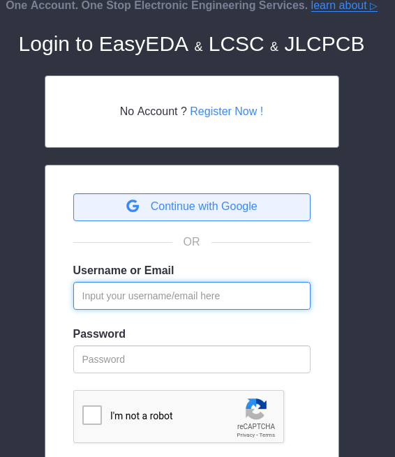
Step 1 : Create an Account in EasyEDA
Go to EasyEDA website and create a free account.

Register and Login using Google Account is also possible.
Step 2 : Start a New Project
Now we will start a new project and start drawing our circuit diagram. Once you are logged in, Go to “Editor”.
File -> New -> Project
Enter the Title, Path and Description and click on save button.
Once a new project is created, to modify your project, right-click on the folder with the project name in the project tree in the left-hand panel, which will open a web page in which you can edit your project.
Step 3: Draw the Circuit / Schematics
Pick and Place the components from the EELib tab from the left panel.
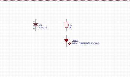
You can also go to libraries, and search for components there. Like I said before, EasyEDA has some cool and powerful drawing tools with which you can create your own symbols either by copying existing symbols into your own library and then editing and saving them, or by drawing them from scratch.
Use “Wire” tool to connect the components together.
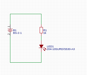
Step 4: Save the Schematics
Once you have finished drawing the circuit, save the circuit by clicking save.
Documents —> Save
Step 5 : Creating Online PCB Layout
Now, from the top tool list, Click on the convert button and Select “Convert to PCB”.
This will open up a window like this.
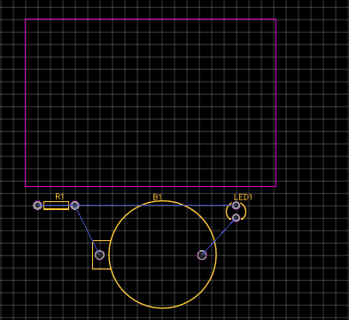
Step 6 : Placing the Components
Here, you can place the components inside the boundary and arrange them the way you want.
To make your PCB to look as clean as possible, It is best to place and route all components with the same function close to each other, like resistors for example.
Once you have finished placing all the components, click save.
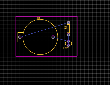
Step 7 : Routing the Components
The easy way route all the component is “auto-route” process.
For that, Click on the “Route” Tool and Select “Auto Router”
This will open up an Auto Router Config Page where you can provide details such as clearance, track width, layer information etc. Once you have done that, click on “Run”.
Thats it guys, you layout is now complete. You can now download the Gerber file and use it to manufacture your PCB from JLCPCB.
This is just a simple example for beginners to get started with. You can create multilayer, complex SMD circuits and get your PCB Layout neat and finished. in minutes.
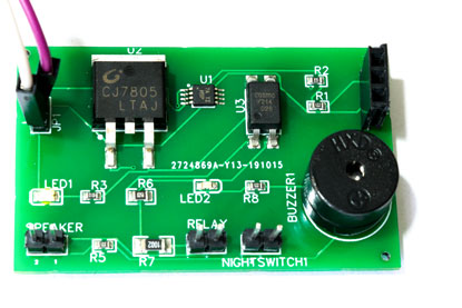
Shown below are some of the cool PCB Layouts Developed using EasyEDA
For more details, check out EasyEDA documentation.
Online PCB Order Step By Step
Follow below steps to order your own PCB from JLCPCB. It wont take more than 1 minute to get everything done.
Step 1 – Create a Free Account
Go to JLC PCBs website and create a free account.

Register and Login using Google Account is also possible.
Step 2 – Upload Gerber File
Once you have successfully created an account, Click on “Quote Now” and upload your Gerber File.
Gerber File contains information about your PCB such as PCB layout information, Layer information, spacing information, tracks to name a few.
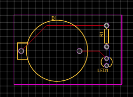
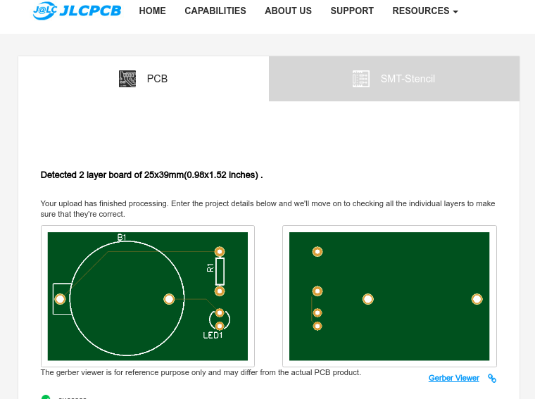
Step 3 – Preview the File
Once the Gerber file is uploaded, it will show you a preview of your circuit board.
Make sure this is the PCB Layout of the board you want.
Step 4 – Choose Necessary PCB Options
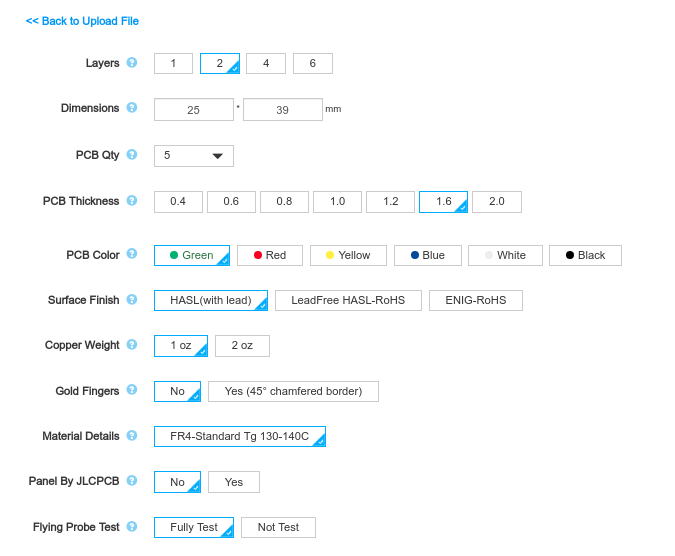
Below the PCB preview, you will see so many options such as PCB Quantity, Texture, Thickness, Color etc. Choose all that are necessary for you.
Step 5 – Checking Out
Once everything is done, click on “Save To Cart”. In the next page, you can choose a shipping and payment option and Check Out Securely. You can either use Paypal or Credit/Debit Card to pay.
The price depends upon the color, size, thickness and quantity.Get Your PCB Done in Minutes!!!CLICK TO TWEET
Thats it guys. Its Done. The PCB will be manufactured and shipped with in days and will be delivered to your doorstep within the mentioned time period.
Overall rating: 4.4 out of 5 based on 220 reviews.
New to Robotics?
We have a beginners guide on “Getting Started with Robotics” which will give you a kick start in this field. Check out our free video tutorial below for a brief introduction.