Eco-Friendly Electronics: The Green PCB Manufacturing!
Green Initiatives in PCB Manufacturing has formed with the goal of revolutionizing the sector through the adoption of eco-friendly procedures, sustainable materials, and ethical waste management.
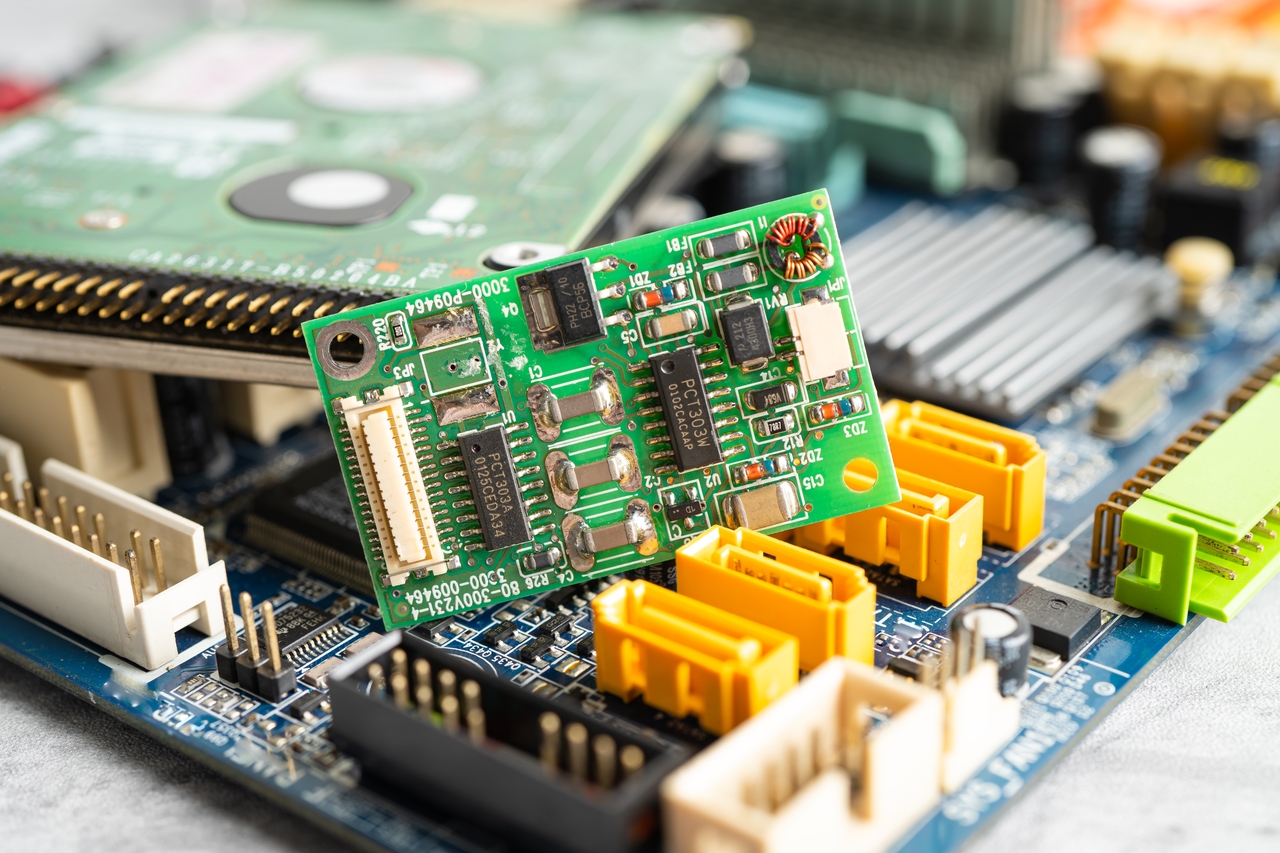
Concern over the effects of electronic gadgets on the environment is developing in a technologically advanced society where they have assimilated into everyday life. The core of electronic gadgets, printed circuit boards (PCBs), are essential to the operation of anything from smartphones to medical equipment. However, the conventional methods for making PCBs frequently use dangerous substances and produce a lot of waste, which presents serious problems for the sustainability of the environment. In response to these worries, a vital movement called “Green Initiatives in PCB Manufacturing” has formed with the goal of revolutionizing the sector through the adoption of eco-friendly procedures, sustainable materials, and ethical waste management. The different approaches and initiatives used to make PCB manufacturing more ecologically friendly are covered in this topic, ensuring that the world we live in is not sacrificed in order to produce the electronics we rely on.
Hazardous Wastes from Traditional PCB Manufacturing
Manufacturing printed circuit boards (PCBs) is a multi-step, chemical and physical process that frequently makes use of potentially dangerous components. Hazardous waste is consequently produced during several stages of PCB manufacture. If these hazardous wastes are not handled and disposed of appropriately, they pose serious dangers to the environment and human health. For successful efforts to reduce their development and ensure responsible waste management, it is essential to understand the sources and potential effects of these wastes.
Unused or wasted materials, such as PCB offcuts and extra laminates, can be produced during PCB production. Incorrect disposal of these things could cause environmental damage and contamination if they contain hazardous elements.
Dross and fumes produced by soldering techniques might include a mixture of metal oxides called dross. Lead, a dangerous heavy metal notorious for damaging the neurological system, especially in young children, is present in dross. Additionally, improper ventilation of soldering vapors can cause the release of hazardous substances like lead and other volatile organic compounds into the air, endangering both the health of workers and the environment.
Besides manufacturing-related hazardous wastes, end-of-life PCBs and electronic waste also significantly contribute to the hazardous waste stream. This is known as waste electrical and electronic equipment (WEEE). When WEEE is disposed of or recycled improperly, dangerous compounds including lead, mercury, and brominated flame retardants may be released, contaminating the environment and perhaps endangering human health.
Waste treatment procedures, such as wastewater treatment or the treatment of chemical wastes, can result in sludge containing heavy metals and other harmful elements. If you want to stop this sludge from leaking into the ground or water sources, you need to dispose of it or treat it properly.
The etching process, a crucial stage in PCB manufacture, involves employing chemical solutions to remove undesired copper from the board. This procedure produces poisonous and caustic chemical wastes such as wasted etchants, which frequently contain ferric chloride or cupric chloride. If not handled appropriately, these chemicals can cause soil and water contamination, damaging aquatic life and perhaps getting into human water systems.
After assembly, PCBs need to be cleaned with chemical cleaning solutions to get rid of impurities like flux smears. Chemical wastes containing solvents and detergents, which can be hazardous to both people and the environment, are produced throughout the cleaning process. These chemical wastes may pollute the air and water if improperly disposed of.
Several tactics can be used to reduce the negative effects that hazardous wastes from PCB manufacture have on the environment:
- Optimizing chemical use, implementing more effective procedures, and implementing cleaner production techniques can all help to limit the production of hazardous waste.
- Research and development efforts can concentrate on locating substitutes that are less hazardous and environmentally benign, hence lowering hazardous waste.
- Investments in efficient waste treatment technology and recycling techniques can assist recover valuable materials and lessen the impact of hazardous wastes.
- To ensure proper processing, transportation, and disposal of hazardous wastes, it is essential to comply with all applicable environmental legislation and standards.
PCB manufacturing produces hazardous pollutants that are extremely harmful to the environment and human health. This problem needs to be addressed holistically, which means encouraging the use of eco-friendly materials, decreasing trash at the source, and implementing ethical waste management procedures. The PCB manufacturing industry may make substantial progress toward environmental sustainability and ensure the welfare of both ecosystems and human populations by giving priority to the reduction and responsible handling of hazardous wastes.
How Green PCB Manufacturing is Beneficial?
Nearly all electronic devices, from cellphones and laptops to medical equipment and automotive systems, depend on printed circuit boards, or PCBs. The demand for environmentally friendly production methods is increasing along with the demand for electronic goods. Green initiatives in the PCB business focus on a variety of issues, from raw materials and production procedures to recycling and waste management, in an effort to lessen the environmental impact of this important sector.
Reduced Waste
The production of waste is a major concern in the PCB industry. Lean manufacturing techniques are used in green projects to eliminate waste while streamlining the production process. The amount of trash ending up in landfills can be greatly decreased by reducing waste generation and putting recycling programs for scrap materials into place.
Extended Producer Responsibility (EPR)
As part of an environmental policy strategy known as extended producer responsibility (EPR), producers are still held accountable for their products long after their useful lives have finished. The rest of the supply chain is now exposed to the idea of a circular strategy as a whole. To create a product more easily recyclable or reusable, designers must consider how the object will be disposed of. This strategy makes producers accountable for every stage of the lifespan of their products. By putting EPR plans into place, PCB producers assume responsibility for the ethical disposal and recycling of their goods, promoting the development of more environmentally friendly production methods.
Green PCB Materials
Utilizing sustainable resources is one of the main components of green PCB manufacturing initiatives. Traditional PCBs frequently contain lead-based solders and brominated flame retardants, both of which are hazardous to the environment and human health. Green PCB production promotes the use of environmentally friendly materials such as recyclable substrates, lead-free laminates, and solder. These eco-friendly materials enhance end-of-life recycling while also reducing hazardous waste.
Water Usage
Several steps in the production of PCBs, including cleaning and etching operations, require water. To reduce water usage and avoid pollution, green programs prioritize responsible water management. You can accomplish this by putting in place water recycling systems and employing eco-friendly cleaning products.
Green Certification
When PCB producers work with governmental entities and environmental organizations, green efforts are more successful. Manufacturers who have earned certifications like ISO 14001, which focuses on environmental management, show their dedication to ethical business practices and sustainability.
Restriction of Hazardous Substances
Compliance with the Restriction of Hazardous Substances (RoHS) directive is essential to green manufacturing activities for PCBs. RoHS limits the use of dangerous materials, especially PCBs, in electronic products, including lead, mercury, cadmium, and some flame retardants. To protect customers and the environment, manufacturers must abide by the RoHS laws.
Circular Economy Approaches
Using the ideas of the circular economy, PCBs can be repaired and refurbished to increase their lifespan. Manufacturers decrease the need for frequent replacements and, as a result, the production of e-waste by encouraging product longevity.
Design for Environment
PCB designers are incorporating Design for Environment principles into their designs. In order to reduce waste and energy usage, design decisions like component location must take the environment into account.
Green Innovations in PCB Manufacturing
Green initiatives in PCB production include the promotion of environmentally sound habits that lessen the ecological footprint of the sector. These programs cover a range of tactics and developments that aim to produce PCBs that are more environmentally friendly and durable. Here are some instances of environmentally friendly PCB manufacturing practices:
Additive PCB Printing
Additive PCB printing technologies eliminate the need for multistep subtractive procedures by utilizing 3D-printed electronics, conformal electronics, aerosol, inkjet, and laserjet printing, as well as direct wire fabrication. Only the materials that are necessary are used in additive manufacturing. For intricate drawings on thin substrates, additive methods work well since they don’t require etchants or photomasks. There is little material waste when PCBs are produced using 3D printing.
Paper PCBs
Multilayer PCBs made of paper are now being made by researchers, which could have substantial positive effects on the environment. A crucial component of electronics is printed circuit boards or PCBs. But a significant portion of electronic waste is made up of PCBs. The paper has generated a lot of curiosity about the assortment of flexible and environmentally acceptable PCB materials. Paper degrades quickly and without any environmental issues. Additionally, it is affordable and versatile. With the roll-to-roll manufacturing method, mass production is feasible.
Lead-Free PCBs
One of the biggest ecological projects in PCB production is the eradication of lead-based solder. To lessen the dangers of electronic waste on the environment and human health, lead-free solder supplies are employed.
Halogen-Free Laminates
Halogen substances, such as brominated flame retardants, are frequently employed in PCBs but they are hazardous to the environment and human health. Halogen-free laminates are encouraged by green efforts as a way to get rid of these dangerous components from PCBs.
These instances show how the PCB manufacturing sector is actively implementing green policies to reduce its environmental impact, encourage resource conservation, and guarantee a more sustainable future for electronics.
Go Green With PCBWay
It’s critical to remember that sustainable practices can be dynamic and ever-changing. Businesses like PCBWay may boost current programs or launch new ones to further demonstrate their commitment to sustainability.
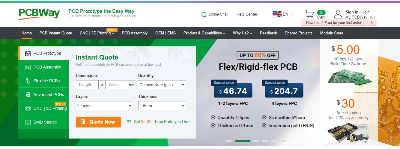
Offering top-notch solutions for the electronics sector, PCBWay is a well-known PCB fabrication and assembly service provider. Delivering high-performance PCBs, flexible PCBs, and PCB assembly services to satisfy a variety of project requirements, PCBWay takes pride in its dedication to innovation and customer satisfaction. The company’s user-friendly web platform makes it simple for consumers to upload their designs and quickly get quotations, which streamlines the purchase process. Environmental concern is seen in PCBWay’s focus on sustainable production methods including lead-free PCBs and RoHS compliance. PCBWay continues to be a reliable partner for people, small businesses, and large enterprises looking for PCB solutions globally because of its team of skilled professionals and cutting-edge manufacturing facilities.
Listed below are a few ways PCBWay has demonstrated its dedication to sustainable production:
Lead-Free PCBs: PCBWay offers lead-free PCB options, aligning with global efforts to eliminate hazardous substances and reduce the environmental impact of electronic waste.
- Halogen-Free Laminates: To address environmental and health concerns related to halogen-containing compounds, PCBWay provides halogen-free laminate options for their PCBs.
- RoHS Compliance: PCBWay ensures that their PCBs comply with the Restriction of Hazardous Substances (RoHS) directive, which restricts the use of hazardous substances in electronic products.
- Energy-Efficient Manufacturing: The company focuses on energy-efficient manufacturing processes, including using energy-saving equipment and optimizing production line layouts to reduce energy consumption.
- Waste Reduction and Recycling: PCBWay implements waste reduction strategies and encourages recycling programs to minimize waste generation and promote responsible waste management.
- Eco-Friendly Materials: The company offers PCB options that utilize eco-friendly materials, contributing to a reduced environmental impact.
- Environmental Certifications: PCBWay may obtain relevant environmental certifications to demonstrate their commitment to sustainable practices and compliance with environmental standards.
- Circular Economy Approaches: PCBWay may support circular economy principles by encouraging PCB repair and refurbishment, thus prolonging the life of PCBs and reducing e-waste.
- Responsible End-of-Life Management: The Company may provide guidance to customers on proper end-of-life management for their PCBs, including recycling options to prevent hazardous materials from being disposed of improperly.
Conclusion
Green PCB manufacturing projects are essential for fostering a more environmentally conscious and sustainable electronics sector. Lead-free PCBs, halogen-free laminates, energy-efficient production, waste reduction, and responsible end-of-life management are just a few examples of eco-friendly techniques that PCB manufacturers may incorporate to drastically lessen their environmental impact and help create a greener, cleaner future. A dedication to moral and sustainable practices can be seen in the adoption of circular economy concepts, a concentration on environmentally friendly products, and adherence to pertinent environmental standards. The pursuit of green efforts in PCB manufacturing is becoming more and more crucial as the demand for electronic gadgets rises in order to protect the environment, conserve resources, and maintain a healthier planet for future generations. The industry takes a proactive step in solving global environmental concerns and providing a good example for other industries to follow by working toward sustainable PCB manufacture.