Less is More: The Impact of Miniaturization of PCBs
A key component of contemporary electrical design and innovation is the continuous trend of printed circuit board (PCB) miniaturization.
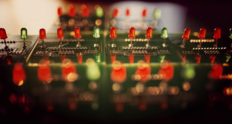
A key component of contemporary electrical design and innovation is the continuous trend of printed circuit board (PCB) miniaturization. PCBs, the circuit boards that power electronic devices, change in tandem with the device’s size, power, and integration to become more sophisticated, efficient, and compact platforms. This trend pushes the envelope in material science and engineering while also advancing a wide range of industries to new heights. The miniaturization of PCBs involves a sophisticated interaction of cutting-edge manufacturing processes, novel materials, and cutting-edge design ideas in addition to shrinking their physical size. This change represents a huge advancement in the rapidly changing field of technology and is essential to fulfilling the increasing need for wearables, IoT devices, and other high-tech applications.
The Impact and Challenges in Miniaturization of PCBs
The electronics industry has been significantly impacted by the miniaturization of printed circuit boards (PCBs), which has changed the way that devices are made, assembled, and utilized. Numerous technological improvements have been made possible by the trend towards smaller, more densely packed PCBs, but there are also several noticeable challenges associated with it.
The trend towards smaller Printed Circuit Boards (PCBs) has enabled a denser packing of components within a limited space, enhancing the power and efficiency of devices. This advancement is particularly significant in sectors like consumer electronics, medical technology, and communication, where the constraints of space and weight are paramount.
This move towards miniaturization has been a catalyst for innovation in various industries. In the field of medical technology, for example, the reduced size of PCBs has facilitated the creation of more streamlined, less invasive devices for both diagnosis and treatment. Similarly, in the aerospace sector, this trend has led to more advanced instrumentation and control systems.
The reduction in PCB size has also revolutionized the portability and wearability of devices, broadening their applications in fitness tracking, health monitoring, and augmented reality, where compactness and convenience are essential. Addressing the various challenges posed by the miniaturization of Printed Circuit Boards (PCBs) is crucial for preserving their functionality and reliability.
When components on PCBs are arranged more compactly, effectively managing the resultant heat poses a considerable challenge, as excessive heat can negatively impact both performance and durability. Therefore, developing innovations in thermal management and heat-dissipating materials becomes essential.
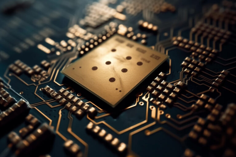
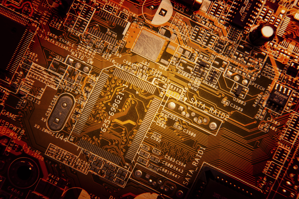
The process of manufacturing PCBs becomes more intricate with miniaturization. This trend demands finer fabrication methods, the use of cutting-edge materials, and enhanced quality control protocols to accommodate the reduced size of components and the narrower margins for error. Furthermore, as component density on PCBs increases, ensuring signal integrity is increasingly difficult. This heightened proximity leads to a greater likelihood of electromagnetic interference (EMI) and signal interference among components, which can diminish device performance.
The design and testing of miniaturized PCBs necessitate sophisticated software and specialized expertise. Testing these compact boards for defects and guaranteeing their long-term reliability presents growing complexities. Lastly, the trend towards smaller PCBs is stretching the capabilities of current materials and components. Continuous research and development in novel materials and microfabrication techniques are essential to address these emerging challenges.
Technologies – Miniaturization of PCBs
Several key technologies have been instrumental in driving the trend of miniaturization in Printed Circuit Boards (PCBs), each contributing significantly to reducing board sizes and boosting their functionality.
Surface Mount Technology (SMT)
The method of mounting components on the surface of a printed circuit board is known as surface mount technology or SMT. For the majority of electronics, the components are made expressly to be directly installed onto the circuit board, as opposed to being hardwired.
Surface Mount Technology (SMT) has revolutionized the field of electronics manufacturing by altering the way Printed Circuit Boards (PCBs) are built and assembled. This modern technology moves away from the conventional through-hole technique, opting instead to mount components directly on the PCB surface, which removes the necessity for inserting leads into holes.
The adoption of SMT results in a markedly increased density of components on PCBs, as it allows for mounting on both sides of the board. This approach negates the need for large lead holes, thus shrinking the PCB’s size and facilitating the creation of smaller, more efficient electronic devices. Components used in SMT are typically smaller, leading to shorter paths for electrical signals and minimizing signal transmission delays. This contributes significantly to the enhanced performance of electronic devices, especially in terms of speed and reliability.
SMT’s highly automated process offers a faster, more economical production method compared to traditional through-hole manufacturing. This efficiency reduces human error, accelerates production rates, and cuts down on costs. PCBs manufactured using SMT generally exhibit greater mechanical strength, particularly under conditions of shaking and vibration. Their reduced size and lower lead inductance also yield improved functionality at higher frequencies.
SMT’s compatibility with a diverse array of electronic components makes it a flexible option for a broad spectrum of electronic devices, ranging from compact consumer products to extensive industrial equipment. Despite its array of benefits, SMT poses certain challenges, such as the need for precise component placement and advanced soldering techniques. Nonetheless, the broad integration of SMT has been instrumental in driving the miniaturization and improved performance of contemporary electronic devices, signifying a major advancement in electronics manufacturing.
High-Density Interconnects (HDI)
High-density interconnects (HDI) represent a notable innovation in the realm of printed circuit board (PCB) design, distinguished by a significantly higher interconnection density than traditional PCBs. Compared to conventional printed circuit boards, high-density interconnect circuit boards have a higher wiring density per unit area.
This advancement plays a crucial role in addressing the contemporary needs of electronic device miniaturization while boosting performance. HDI boards feature an elevated density of vias—tiny holes facilitating layer-to-layer connections—and more compact conductive pathways. This higher density is key to incorporating more functionalities into a single board, vital for crafting smaller electronic devices such as smartphones, tablets, and medical equipment.
In HDI design, the use of micro vias, which are much smaller than standard vias, is common. These microvias, either blind or buried, enable more intricate routing and layering in PCB design, allowing for greater complexity. The condensed structure of HDI PCBs shortens signal paths and reduces signal loss and interference, leading to quicker signal transmission and superior electrical performance, especially important in high-speed and frequency applications.
HDI’s capacity to merge several traditional PCB layers into one reduces the size and weight of the final electronic device, a significant advantage in sectors where compactness and lightness are essential, such as aerospace and portable electronics. Although initially more costly due to the intricate precision and complexity involved in their production, HDI boards can be more economical over time. The integration of multiple functionalities into a single board reduces the need for multiple separate boards, cutting overall costs.
The design and production of HDI PCBs demand high-level technology and expertise. Their detailed features and compact designs require exacting fabrication processes and thoughtful design planning to ensure both reliability and manufacturability.
Flexible PCB
A flexible printed circuit board consists of many printed circuits assembled on a flexible substrate, together with additional components. It’s similar to a regular rigid circuit board in terms of components, but it’s designed to be flexible, letting it bend to fit the needed shape during its use. The materials used to make flex PCBs are typically polyimide or related polymers, which can bend and flex. These materials can tolerate the strains of bending and flexing because they are strong and flexible.
Flex PCBs can flex when being applied, and they can fit into locations that rigid PCBs cannot. This makes them perfect for intricate or small-sized electronic devices including wearables, medical equipment, smartphones, and aeronautical technology. The most basic and versatile kind of flex circuits are single-sided ones, which consist of a single layer of conductive material. More circuit density is possible with Double-Sided Flex Circuits, which contain two conducting layers that can be joined by plated through-holes.
With numerous layers of conductive material, Multilayer Flex Circuits provide a higher circuit density and more intricate design. Rigid-flex circuits combine the advantages of flexible and rigid PCB technologies into a single circuit. Usually, they are utilized in more intricate electronic applications. Flex PCBs are perfect for today’s tiny gadgets since they are lighter and more space-efficient. Because it can bend without breaking the circuitry, the material is under less stress, which extends the product’s lifespan. Flex PCBs can dissipate heat more effectively than stiff PCBs in some designs.
Flex PCB manufacture is a more sophisticated process than that of rigid PCBs, frequently involving specialized tools and knowledge. Their production cost may increase as a result. Consumer electronics (such as cameras and cellphones), automotive (particularly in small places or with moving parts), medical devices (because of their flexibility and lightweight), and industrial applications are just a few of the many uses for flex PCBs.
Rigid Flex PCB
Rigid-flex PCBs are a hybrid form of circuit boards that incorporate the properties of both rigid and flexible PCBs (Printed Circuit Boards). A special set of benefits and applications are made possible by this combination. Layers of rigid PCBs joined by layers of flexible PCBs make up rigid-flex PCBs. Complex three-dimensional designs are made possible by the flexible sections that may bend and move, while the rigid components offer the stability and density of a conventional PCB.
Usually composed of conductive copper layers, the flexible layers are built of a flexible, high-temperature plastic like polyimide. Similar to regular rigid PCBs, the stiff parts are frequently composed of FR4. It is possible to fold or bend rigid-flex PCBs to make them fit into tight or asymmetrical places. They are perfect for applications where weight is an issue because they are usually lighter than conventional rigid PCBs. Because it is flexible to install, fewer connectors and wires are required, which lowers the possibility of failure sites. 3D Connectivity makes it possible to design compact and more imaginative products.
Numerous industries, including aerospace, military, medical, consumer electronics (such as smartphones and cameras), and automotive electronics, use rigid-flex printed circuit boards. They are especially useful in situations when electronic parts have to push themselves into small or oddly shaped areas. The main benefit of using rigid-flex printed circuit boards is their capacity to build extremely intricate, multi-layered electronic circuits. In situations when there is a shortage of room and the electronics must move or take on a certain shape, they are especially helpful.
Because rigid-flex circuit boards require careful planning of the layout to accommodate both rigid and flexible sections, their production is more complex than that of regular PCBs. This intricacy frequently results in increased production and design expenses. Because of the intricate manufacturing process and the requirement for exact alignment of the rigid and flexible components, designing and producing Rigid-Flex PCBs can be difficult. When compared to ordinary PCBs, this complexity may result in increased prices.
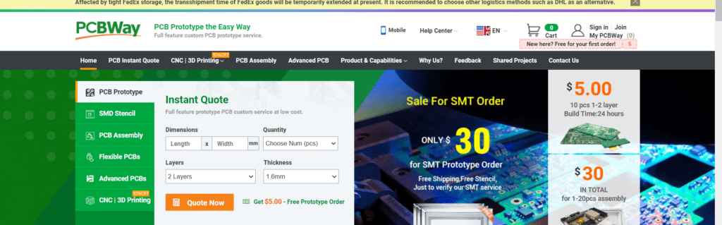
PCBWay in Miniaturization of PCBs
PCBWay has been instrumental in advancing the miniaturization of printed circuit boards (PCBs), offering an array of services and technologies tailored to this growing need. Known for its diverse manufacturing capabilities, PCBWay produces various PCB types, such as rigid, aluminum, copper, flexible, and rigid-flex PCBs, each meeting specific demands in the trend towards smaller electronic components.
In the realm of miniaturized electronics, rigid-flex PCBs have gained particular prominence, favored for their dual characteristics. They merge the rigidity of standard PCBs with the adaptability of flexible ones, enabling the creation of compact, lightweight devices with enhanced functionality. This makes them ideal for a range of sectors, including wearable tech, medical equipment, automotive systems, and Internet of Things (IoT) applications. PCBWay’s expertise in producing rigid-flex PCBs involves handling intricate designs with precision and quality, offering customization to meet varied project needs.
PCBWay’s services extend beyond manufacturing, covering the entire process from initial prototyping to final assembly. Their prototyping service is notable for its versatility, offering choices in shapes, sizes, and complexities, along with a variety of base materials and design options. The subsequent assembly phase is crucial, entailing detailed procedures like solder paste application, component placement, and soldering, typically performed by machines for enhanced precision and efficiency.
Quality assurance is a cornerstone of PCBWay’s operations, underscored by its use of premium materials and adherence to ISO 9001 and UL certifications. Additionally, PCBWay fosters a vibrant community of over a quarter-million users, promoting a collaborative space for sharing projects and expertise. This community engagement is further enhanced through regular events, such as shopping festivals and giveaways, which benefit both PCBWay and its members.
Overall, PCBWay’s comprehensive approach, encompassing a broad spectrum of services, a commitment to quality, and robust community engagement, positions it as a key figure in the PCB manufacturing industry, particularly in the field of advanced and miniaturized PCB technologies.
Conclusion
A major development in electronics engineering, the miniaturization of PCBs (Printed Circuit Boards) reflects the continuous trend towards smaller, more efficient, and highly integrated technologies. The increasing need for contemporary electronics for compactness, lower power consumption, and improved performance have fueled this growth. The creation of rigid-flex PCBs and other advancements in PCB design have been essential in permitting this miniaturization. The possibilities for many industries have expanded as a result of these technical advancements, including consumer electronics, medical gadgets, automotive systems, and more. With businesses like PCBWay and others pushing the limits of PCB technology and providing sophisticated manufacturing capabilities and all-inclusive services, electronics will likely get even smaller, more effective, and more versatile in the future, with a great deal of room for future technological advancements.